D R McCoy

Who am I?

Computer science, human–computer interaction. Student @ Victoria University of Wellington.

I'm a student at Victoria University of Wellington studying a Bachelor of Design Innovation, majoring in interaction design and computer science with a minor in industrial design. Before university I spent several years in electrical trade work. I work across hardware, software and interaction design. This site is one example.

Hellomy name is

D R McCoy

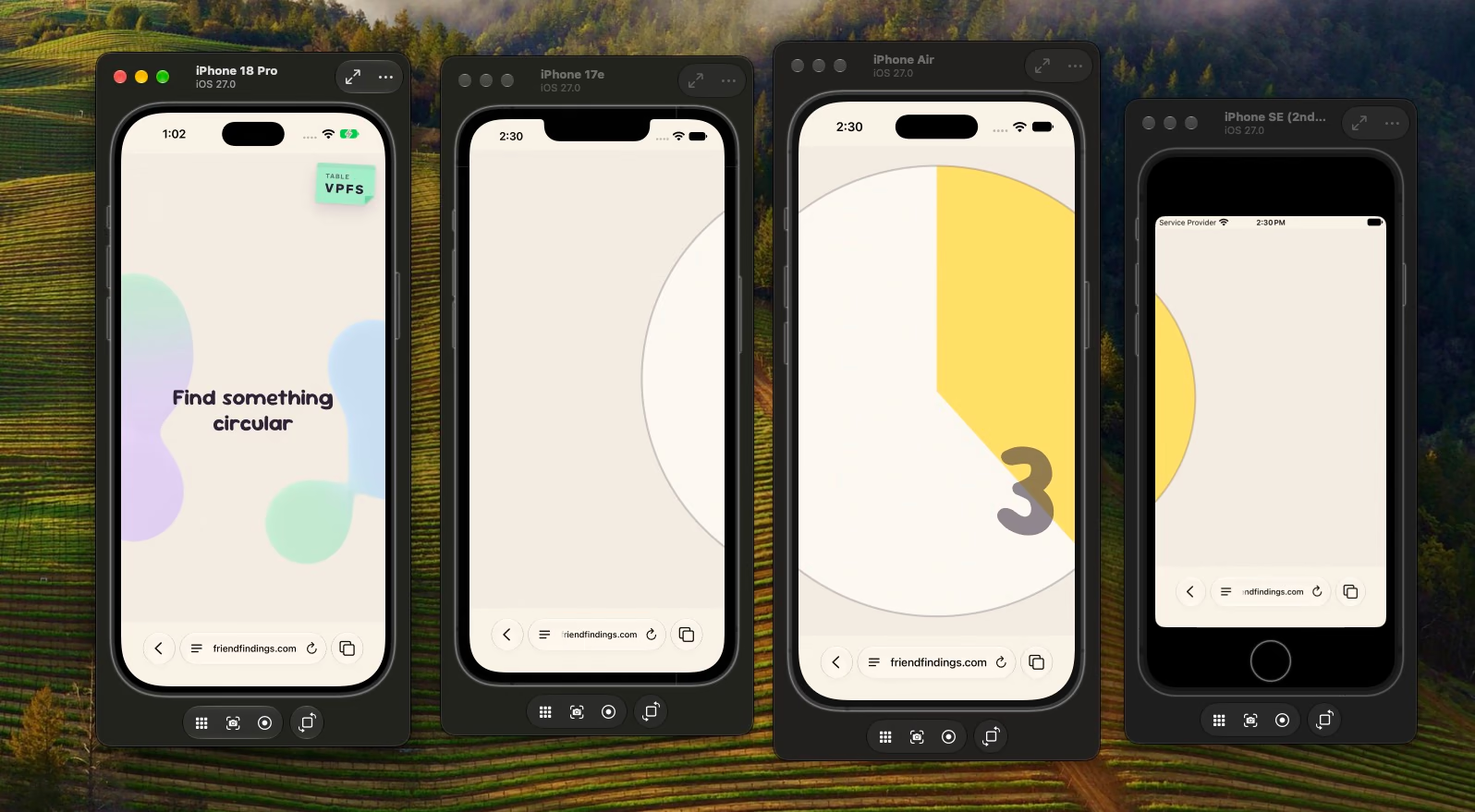
Host phone showing the task and three player phones showing the countdown
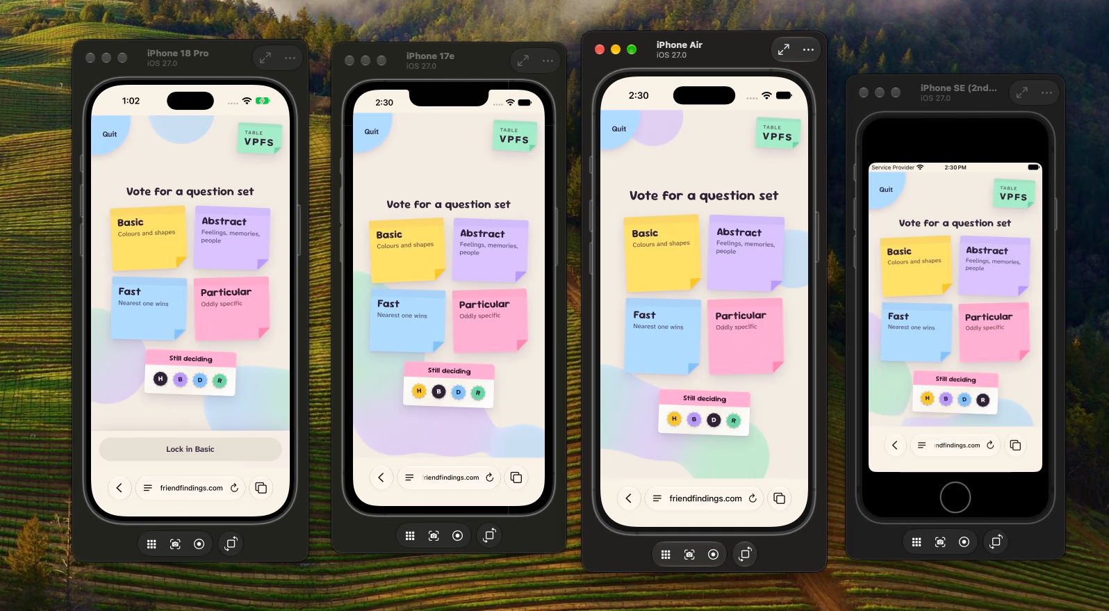
Four phone simulators showing the question-set vote
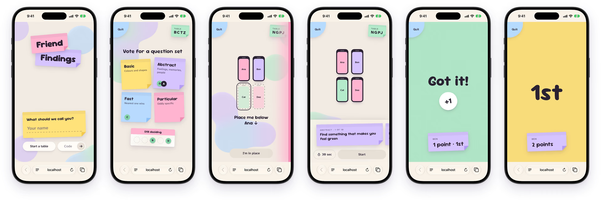
Six phone screens showing joining, voting, placement, scoring and final results
Watermarked output
Residual signal amplified 10x
Cover image

D R MCCOY

WELLINGTON, NEW ZEALAND

RECEIPT FOR YOUR VISIT

PRIVACY · LICENCES · CREDITS

ORDERBCC7513

PRINTED05 OCT 2026

BILLED TOYOU, THE VISITOR

COOKIES00.00

ANALYTICS00.00

TRACKERS00.00

PERSONAL DATA00.00

TYPEFACES60.00

TOTAL0.00

STATUSN/C

HOSTCLOUDFLARE.

TYPEATKINSON HYPERLEGIBLE NEXT

& MONO. BRAILLE INSTITUTE,

SIL OPEN FONT LICENSE.

CAVEAT. THE CAVEAT PROJECT

AUTHORS, SIL OPEN FONT

LICENSE.

NEW COMPUTER MODERN & MONO,

GUST FONT LICENSE.

COURIER PRIME,

SIL OPEN FONT LICENSE.

WORKWORDS, IMAGES AND PROJECTS

© 2026 D R MCCOY.

ALL RIGHTS RESERVED.

MARKSGITHUB, HUGGING FACE AND

ARE.NA MARKS ARE THEIR

OWNERS'.

***

THANK YOU FOR VISITING.

Ambient synth

D R McCoy
This was a project for Physical computing at university, images and more info to come.

Schematics

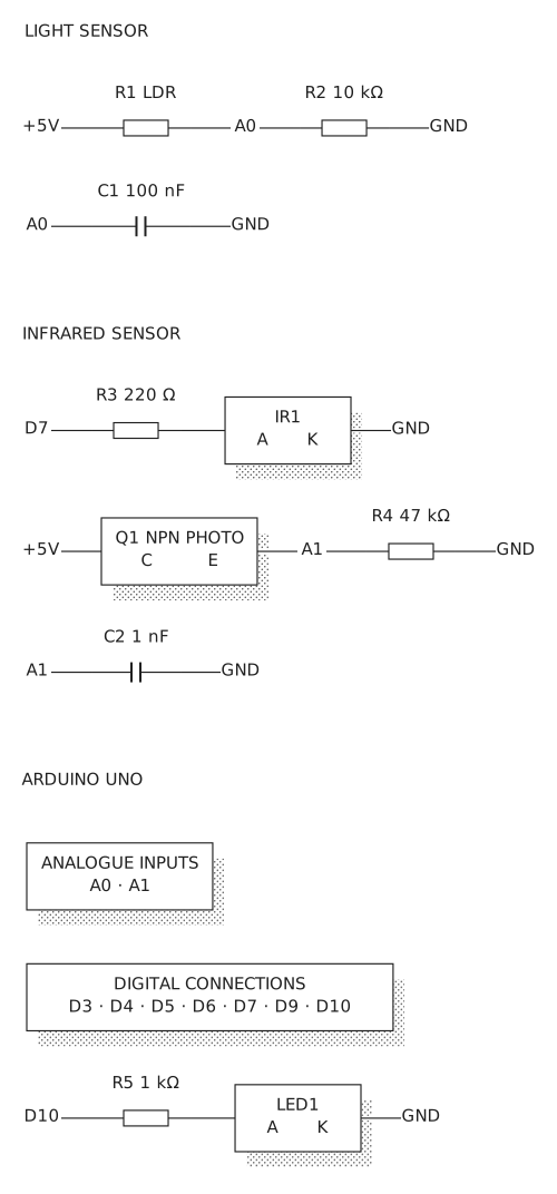
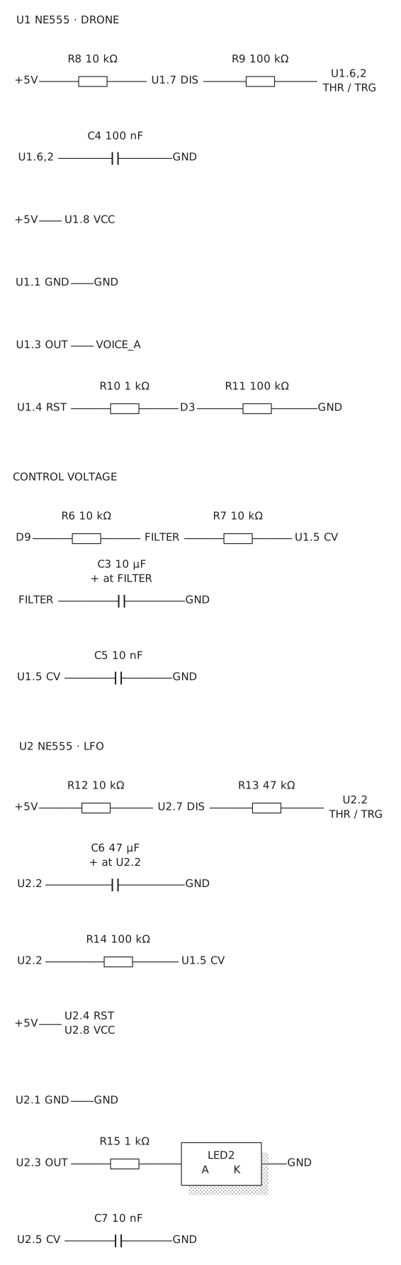
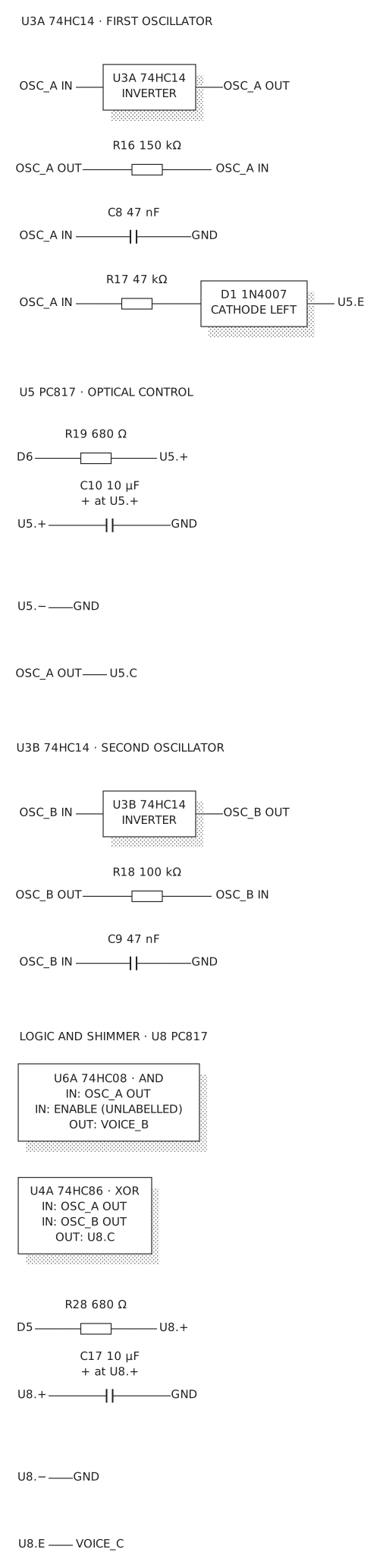
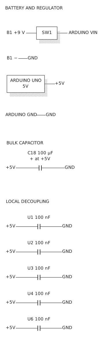
Matching terminal labels indicate an electrical connection. Components without a dedicated symbol are shown as labelled blocks.

01 · Sensors and Arduino

Sensors and ArduinoIdentical terminal labels are connected. Component values and terminal names follow the original schematic. Components without a dedicated Stipple symbol are labelled blocks.LIGHT SENSOR+5VR1 LDRA0R2 10 kΩGNDA0C1 100 nFGNDINFRARED SENSORD7R3 220 ΩIR1A KGND+5VQ1 NPN PHOTOC EA1R4 47 kΩGNDA1C2 1 nFGNDARDUINO UNOANALOGUE INPUTSA0 · A1DIGITAL CONNECTIONSD3 · D4 · D5 · D6 · D7 · D9 · D10D10R5 1 kΩLED1A KGNDOpen full-size diagram

02 · Drone and LFO

Drone and LFOIdentical terminal labels are connected. Component values and terminal names follow the original schematic. Components without a dedicated Stipple symbol are labelled blocks.U1 NE555 · DRONE+5VR8 10 kΩU1.7 DISR9 100 kΩU1.6,2THR / TRGU1.6,2C4 100 nFGND+5VU1.8 VCCU1.1 GNDGNDU1.3 OUTVOICE_AU1.4 RSTR10 1 kΩD3R11 100 kΩGNDCONTROL VOLTAGED9R6 10 kΩFILTERR7 10 kΩU1.5 CVFILTERC3 10 µF+ at FILTERGNDU1.5 CVC5 10 nFGNDU2 NE555 · LFO+5VR12 10 kΩU2.7 DISR13 47 kΩU2.2THR / TRGU2.2C6 47 µF+ at U2.2GNDU2.2R14 100 kΩU1.5 CV+5VU2.4 RSTU2.8 VCCU2.1 GNDGNDU2.3 OUTR15 1 kΩLED2A KGNDU2.5 CVC7 10 nFGNDOpen full-size diagram

03 · Melody and shimmer

Melody and shimmerIdentical terminal labels are connected. Component values and terminal names follow the original schematic. Components without a dedicated Stipple symbol are labelled blocks. The unlabelled enable terminal is retained as unlabelled. U5 and U8 are PC817 optocouplers; C and E name their transistor terminals.U3A 74HC14 · FIRST OSCILLATOROSC_A INU3A 74HC14INVERTEROSC_A OUTOSC_A OUTR16 150 kΩOSC_A INOSC_A INC8 47 nFGNDOSC_A INR17 47 kΩD1 1N4007CATHODE LEFTU5.EU5 PC817 · OPTICAL CONTROLD6R19 680 ΩU5.+U5.+C10 10 µF+ at U5.+GNDU5.−GNDOSC_A OUTU5.CU3B 74HC14 · SECOND OSCILLATOROSC_B INU3B 74HC14INVERTEROSC_B OUTOSC_B OUTR18 100 kΩOSC_B INOSC_B INC9 47 nFGNDLOGIC AND SHIMMER · U8 PC817U6A 74HC08 · ANDIN: OSC_A OUTIN: ENABLE (UNLABELLED)OUT: VOICE_BU4A 74HC86 · XORIN: OSC_A OUTIN: OSC_B OUTOUT: U8.CD5R28 680 ΩU8.+U8.+C17 10 µF+ at U8.+GNDU8.−GNDU8.EVOICE_COpen full-size diagram

03b · Melody, as wired

Melody, as wiredIdentical terminal labels are connected. Component values and terminal names follow the original schematic. Components without a dedicated Stipple symbol are labelled blocks. The open U5 emitter and diode branch are retained from the as-wired drawing; they are not joined. U5 and U8 are PC817 optocouplers.U3 74HC14 · OSCILLATORSU3.1U3AINVERTERU3.2U3.2R16 150 kΩU3.1U3.1C8 47 nFGNDU3.3U3BINVERTERU3.4U3.4R18 100 kΩU3.3U3.3C9 47 nFGNDU5 PC817 · AS WIREDD6R19 680 ΩU5.+U5.+C10 10 µF+ at U5.+GNDU5.−GNDU5.CU3.2U5.EOPENU3.1R17 47 kΩD1 1N4007CATHODE LEFTOPENU4 74HC86 · XORU3.2U4.1U3.4U4.2U4A 74HC86 · XORIN: U4.1 · U4.2OUT: U4.3U4.3U8.CU6 74HC08 · ANDU3.2U6.1D4U6.2U6A 74HC08 · ANDIN: U6.1 · U6.2OUT: U6.3 / VOICE_BU8 PC817 · SHIMMERD5R28 680 ΩU8.+U8.+C17 10 µF+ at U8.+GNDU8.−GNDU8.EVOICE_CIC POWER+5VU3.14 · U4.14 · U6.14GNDU3.7 · U4.7 · U6.7Open full-size diagram

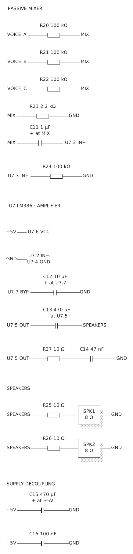
04 · Mixer, amplifier, speakers

Mixer, amplifier, speakersIdentical terminal labels are connected. Component values and terminal names follow the original schematic. Components without a dedicated Stipple symbol are labelled blocks.PASSIVE MIXERVOICE_AR20 100 kΩMIXVOICE_BR21 100 kΩMIXVOICE_CR22 100 kΩMIXMIXR23 2.2 kΩGNDMIXC11 1 µF+ at MIXU7.3 IN+U7.3 IN+R24 100 kΩGNDU7 LM386 · AMPLIFIER+5VU7.6 VCCGNDU7.2 IN−U7.4 GNDU7.7 BYPC12 10 µF+ at U7.7GNDU7.5 OUTC13 470 µF+ at U7.5SPEAKERSU7.5 OUTR27 10 ΩC14 47 nFGNDSPEAKERSSPEAKERSR25 10 ΩSPK18 ΩGNDSPEAKERSR26 10 ΩSPK28 ΩGNDSUPPLY DECOUPLING+5VC15 470 µF+ at +5VGND+5VC16 100 nFGNDOpen full-size diagram

05 · Power

PowerIdentical terminal labels are connected. Component values and terminal names follow the original schematic. Components without a dedicated Stipple symbol are labelled blocks. The 100 nF decoupling capacitors retain their IC labels from the original drawing.BATTERY AND REGULATORB1 +9 VSW1ARDUINO VINB1 −GNDARDUINO UNO5V+5VARDUINO GNDGNDBULK CAPACITOR+5VC18 100 µF+ at +5VGNDLOCAL DECOUPLING+5VU1 100 nFGND+5VU2 100 nFGND+5VU3 100 nFGND+5VU4 100 nFGND+5VU6 100 nFGNDOpen full-size diagram

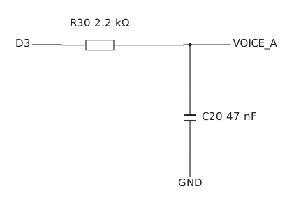
06 · PWM DAC filter

PWM DAC filterD3 feeds VOICE_A through R30, 2.2 kΩ. C20, 47 nF, connects VOICE_A to ground.D3R30 2.2 kΩVOICE_AC20 47 nFGNDOpen full-size diagram